Showing posts with label SWITCHES. Show all posts

Monday, 12 December 2016

SILICON CONTROLLED RECTIFIER

                           SILICON CONTROLLED RECTIFIER
A silicon controlled rectifier or semiconductor-controlled rectifier is a four-layer solidstate current-controlling device. The name "silicon controlled rectifier" is General Electric's trade name for a type of thyristor.
SCRs are mainly used in electronic devices that require control of high voltage and power. This makes them applicable in medium and high AC power operations such as motor control function.

An SCR conducts when a gate pulse is applied to it, just like a diode. It has four layers of semiconductors that form two structures namely; NPNP or PNPN. In addition, it has three junctions labeled as J1, J2 and J3 and three terminals(anode, cathode and a gate). An SCR is diagramatically represented as shown below.
                                                    
The anode connects to the P-type, cathode to the N-type and the gate to the P-type as shown below.
                                                     
In an SCR, the intrinsic semiconductor is silicon to which the required dopants are infused. However, doping a PNPN junction is dependent on the SCR application.

Modes of Operation in SCR

·        OFF state (forward blocking mode) − Here the anode is assigned a positive voltage, the gate is assigned a zero voltage (disconnected) and the cathode is assigned a negative voltage. As a result, Junctions J1 and J3 are in forward bias while J2 is in reverse bias. J2 reaches its breakdown avalanche value and starts to conduct. Below this value, the resistance of J1 is significantly high and is thus said to be in the off state.
·        ON state (conducting mode) − An SCR is brought to this state either by increasing the potential difference between the anode and cathode above the avalanche voltage or by applying a positive signal at the gate. Immediately the SCR starts to conduct, gate voltage is no longer needed to maintain the ON state and is, therefore, switched off by −
o   Decreasing the current flow through it to the lowest value called holding current
o   Using a transistor placed across the junction.
         Reverse blocking − This compensates the drop in forward voltage. This is due to the fact that a low doped region in P1 is needed. It is important to note that the voltage ratings of forward and reverse blocking are equal.
DECLARATION:
OUR BLOG IS NOT FOR COMMERCIAL PURPOSE.ONLY FOR EDUCATIONAL PURPOSE.ALL CREDITS GOES TO BLOG AND RESPECTIVE AUTHOR.CLICK HERETO GO ORGINAL PAGE.

ELECTRONIC SWITCHING

                                     ELECTRONIC SWITCHING


A power electronic switching device is a combination of active switchable power semiconductor drivers that have been integrated into one. The main characteristics of the switch are determined by internal correlation of functions and interactions of its integrated system. The figure given below shows how a power electronic switch system works.
The external circuit of the above diagram is usually held at a high potential relative to the control unit. Inductive transmitters are used to support the required potential difference between the two interfaces.
Power switching devices are normally selected based on the rating at which they handle power, that is, the product of their current and voltage rating instead of their power dissipation rate. Consequently, the major attractive feature in a power electronic switch is its capability to dissipate low or almost no power. As a result, the electronic switch able to achieve a low and continuous surge of power.


DECLARATION:
OUR BLOG IS NOT FOR COMMERCIAL PURPOSE.ONLY FOR EDUCATIONAL PURPOSE.ALL CREDITS GOES TO BLOG AND RESPECTIVE AUTHOR.CLICK HERETO GO ORGINAL PAGE.

Sunday, 11 December 2016

Thyristor Application

Thyristor Application Types Construction Principle of Thyristor
A thyristor is normally four layer three-terminal device. Four layers are formed by alternating n-type and p-type semiconductor materials. Consequently there are three p-n junctions formed in the device. It is a bistable device. The three terminals of this device are called anode (A), cathode (K) and gate (G) respectively. The gate (G) terminal is control terminal of the device. That means, the current flowing through the device is controlled by electrical signal applied to the gate (G) terminal. The anode (A) and cathode (K) are the power terminals of the device handle the large applied voltage and conduct the major current through the thyristor. For example, when the device is connected in series with load circuit, the load current will flow through the device from anode (A) to cathode (K) but this load current will be controlled by the gate(G) signal applied to the device externally. A tyristor is on-off switch which is used to control output power of an electrical circuit by switching on and off the load circuit periodically in a preset interval. The main difference of thyristors with other digital and electronics switches is that, a thyristor can handle large current and can withstand large voltage, whereas other digital and electronic switches handle only tiny current and tiny voltage.
When positive potential applied to the anode with respect to the cathode, ideally no current will flow through the device and this condition is called forward – blocking state but when appropriate gate signal is applied, a large forward anode current starts flowing, with a small anode–cathode potential drop and the device becomes in forward-conduction state. Although after removing the gate signal, the device will remain in its forward-conduction mode until the polarity of the load reverses. Some thyristors are also controllable in switching from forward-conduction back to a forward-blocking state.
Application of Thyristor
As we already said that a thyristor is designed to handle large current and voltage, it is used mainly in electrical power circuit with system voltage more than 1 kV or currents more than 100 A. The main advantage of using thyristors as power control device is that as the power is controlled by periodic on-off switching operation hence (ideally) there is no internal power loss in the device for controlling power in output circuit. Thyristors are commonly used in some alternating power circuits to control alternating output power of the circuit to optimize internal power loss at the expense of switching speed.
In this case thyristors are turned from forward-blocking into forward-conducting state at some predetermined phase angle of the input sinusoidal anode-cathode voltage waveform. Thyristors are also very popularly used in inverter for converting direct power to alternating power of specified frequency. These are also used in converter to convert an alternating power into alternating power of different amplitude and frequency.This is the most common application of thyristor.
Types of Thyristors
There are four major types of thyristors:
1.  Silicon Controlled Rectifier (SCR);
2.  Gate Turn-off Thyristor (GTO) and Integrated Gate Commutated Thyristor (IGCT);
3.  MOS-Controlled Thyristor (MCT)
4.  Static Induction Thyristor (SITh).
Basic Construction of Thyristor
A high- resistive, n-base region, presents in every thyristor. As it is seen in the figure, this n-base region is associated with junction, J2. This must support the large applied forward voltages that occur when the switch is in its off- or forward-blocking state (non-conducting). This n-base region is typically doped with impurity phosphorous atoms at a concentration of 1013 to 1014 per cube centimeter. This region is typically made 10 to 100 micrometer thick to support large voltages. High-voltage thyristors are generally made by diffusing aluminum or gallium into both surfaces to create p-doped regions forming deep junctions with the n-base. The doping profile of the p-regions ranges from about 1015 to 1017 per cube centimeter. These p-regions can be up to tens of micrometer thick. The cathode region (typically only a few micrometer thick) is formed by using phosphorous atoms at a doping density of 1017 to 1018 cube centimeter. For higher forward-blocking voltage rating of thyristor, the n-base region is made thicker. But thicker n - based high-resistive region slows down on off operation of the device. This is because of more stored charge during conduction. A device rated for forward blocking voltage of 1 kV will operate much more slowly than the thyristor rated for 100 V. Thicker high-resistive region also causes larger forward voltage drop during conduction. Impurity atoms, such as platinum or gold, or electron irradiation are used to create charge-carrier recombination sites in the thyristor. The large number of recombination sites reduces the mean carrier lifetime (average time that an electron or hole moves through the Si before recombining with its opposite charge-carrier type). A reduced carrier lifetime shortens the switching times (in particular the turn-off or recovery time) at the expense of increasing the forward-conduction drop. There are other effects associated with the relative thickness and layout of the various regions that make up modern thyristors, but the major trade off between forward-blocking voltage rating and switching times and between forward-blocking voltage rating and forward-voltage drop during conduction should be kept in mind. (In signal-level electronics an analogous trade off appears as a lowering of amplification (gain) to achieve higher operating frequencies, and is often referred to as the gain-bandwidth product.)
Basic Operating Principle of Thyristor
Although there are different types of thyristors but basic operating principle of all thyristor more or less same. The figure below represents a conceptual view of a typical thyristor. There are three p–n junctions J1, J2 and J3. There are also three terminals anode (A), cathode (K) and gate (G) as levelled in the figure. When the anode (A) is in higher potential with respect to the cathode, the junctions J1 and J3 are forward biased and J2 is reverse biased and the thyristor is in the forward blocking mode. A thyristor can be considered as back to back connected two bipolar transistors. A p-n-p-n structure of thyristor can be represented by the p-n-p and n-p-n transistors, as shown in the figure. Here in this device, the collector current of one transistor is used as base current of other transistor. When the device is in forward blocking mode if a hole current is injected through the gate (G) terminal, the device is triggered on.
schematic diagram of thyristor
When potential is applied in reverse direction, the thyristor behaves as a reverse biased diode. That means it blocks current to flow in revere direction. Considering ICO to be the leakage current of each transistor in cut-off condition, the anode current can be expressed in terms of gate current. Where α is the common base current gain of the transistor (α = IC/IE). The anode current becomes arbitrarily large as (α1 + α2) approaches unity. As the anode–cathode voltage increases, the depletion region expands and reduces the neutral base width of the n1 and p2 regions. This causes a corresponding increase in the α of the two transistors. If a positive gate current of sufficient magnitude is applied to the thyristor, a significant amount of electrons will be injected across the forward-biased junction, J3, into the base of the n1p2n2 transistor. The resulting collector current provides base current to the p1n1p2 transistor. The combination of the positive feedback connection of the npn and pnp BJTs and the current-dependent base transport factors eventually turn the thyristor on by regenerative action. Among the power semiconductor devices known, the thyristor shows the lowest forward voltage drop at large current densities. The large current flow between the anode and cathode maintains both transistors in saturation region, and gate control is lost once the thyristor latches on.
Transient Operation of Thyristor

A thyristor is not turned on as soon as the gate current is injected, there is one minimum time delay is required for regenerative action. After this time delay, the anode current starts rising rapidly to on-state value. The rate of rising of anode current can only be limited by external current elements. The gate signal can only turn on the thyristor but it cannot turn off the device. It is turned off naturally when the anode current tends to flow in reverse direction during the reverse cycle of the alternating current. A thyristor exhibits turn-off reverse recovery characteristics just like a diode. Excess charge is removed once the current crosses zero and attains a negative value at a rate determined by external circuit elements. The reverse recovery peak is reached when either junction J1 or J3 becomes reverse biased. The reverse recovery current starts decaying, and the anode-cathode voltage rapidly attains its off-state value. Because of the finite time required for spreading or collecting the charge plasma during turn-on or turn-off stage, the maximum dI/dt and dV/dt that may be imposed across the device are limited in magnitude. Further, device manufacturers specify a circuit-commutated recovery time, for the thyristor, which represents the minimum time for which the thyristor must remain in its reverse blocking mode before forward voltage is reapplied.

DECLARATION:
OUR BLOG IS NOT FOR COMMERCIAL PURPOSE.ONLY FOR EDUCATIONAL PURPOSE.ALL CREDITS GOES TO BLOG AND RESPECTIVE AUTHOR.CLICK HERETO GO ORGINAL PAGE.

TRIAC

TRIAC
triac
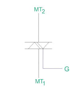
Triac is a three terminal AC switch which is different from the other silicon controlled rectifiers in the sense that it can conduct in both the directions that is whether the applied gate signal is positive or negative, it will conduct. Thus, this device can be used for AC systems as a switch.This is a three terminal, four layer, bi-directional semiconductor device that controls AC power. The triac of maximum rating of 16 kw is available in the market. Figure shows the symbol of triac, which has two main terminals MT1 and MT2 connected in inverse parallel and a gate terminal.
Construction of Triac
construction of a triac
Two SCRs are connected in inverse parallel with gate terminal as common. Gate terminals is connected to both the N and P regions due to which gate signal may be applied which is irrespective of the polarity of the signal. Here, we do not have anode and cathode since it works for both the polarities which means that device is bilateral. It consists of three terminals namely, main terminal 1(MT1), main terminal 2(MT2), and gate terminal G. Figure shows the construction of a triac. There are two main terminals namely MT1 and MT2 and the remaining terminal is gate terminal.
Operation of Triac
The triac can be turned on by applying the gate voltage higher than break over voltage. However, without making the voltage high, it can be turned on by applying the gate pulse of 35 micro seconds to turn it on. When the voltage applied is less than the break over voltage, we use gate triggering method to turn it on. There are four different modes of operations, they are-
1.  When MT2 and Gate being Positive with Respect to MT1 When this happens, current flows through the path P1-N1-P2-N2. Here, P1-N1 and P2-N2 are forward biased but N1-P2 is reverse biased. The triac is said to be operated in positively biased region. Positive gate with respect to MT1 forward biases P2-N2 and breakdown occurs.
2.  When MT2 is Positive but Gate is Negative with Respect to MT1 The current flows through the path P1-N1-P2-N2. But P2-N3 is forward biased and current carriers injected into P2 on the triac.
3.  When MT2 and Gate are Negative with Respect to MT1 Current flows through the path P2-N1-P1-N4. Two junctions P2-N1 and P1-N4 are forward biased but the junction N1-P1 is reverse biased. The triac is said to be in the negatively biased region.
4.  When MT2 is Negative but Gate is Positive with Respect to MT1 P2-N2 is forward biased at that condition. Current carriers are injected so the triac turns on. This mode of operation has a disadvantage that it should not be used for high (di/dt) circuits. Sensitivity of triggering in mode 2 and 3 is high and if marginal triggering capability is required, negative gate pulses should be used. Triggering in mode 1 is more sensitive than mode 2 and mode 3.
Characteristics of a Triac
The triac characteristics is similar to SCR but it is applicable to both positive and negative triac voltages. The operation can be summarized as follows-  
First Quadrant Operation of Triac
Voltage at terminal MT2 is positive with respect to terminal MT1 and gate voltage is also positive with respect to first terminal.
Second Quadrant Operation of Triac
Voltage at terminal 2 is positive with respect to terminal 1 and gate voltage is negative with respect to terminal 1.
Third Quadrant Operation of Triac
Voltage of terminal 1 is positive with respect to terminal 2 and the gate voltage is negative.
Fourth Quadrant Operation of Triac
v-i characteristics of a triac
Voltage of terminal 2 is negative with respect to terminal 1 and gate voltage is positive. When the device gets turned on, a heavy current flows through it which may damage the device, hence in order to limit the current a current limiting resistor should be connected externally to it. By applying proper gate signal, firing angle of the device may be controlled. The gate triggering circuits should be used for proper gate triggering. We can use diac for triggering the gate pulse. For firing of the device with proper firing angle, a gate pulse may be applied up to a duration of 35 micro seconds.
Advantages of Triac
1.  It can be triggered with positive or negative polarity of gate pulses.
2.  It requires only a single heat sink of slightly larger size, whereas for SCR, two heat sinks should be required of smaller size.
3.  It requires single fuse for protection.
4.  A safe breakdown in either direction is possible but for SCR protection should be given with parallel diode.
Disadvantages of Triac
1.  They are not much reliable compared to SCR.
2.  It has (dv/dt) rating lower than SCR.
3.  Lower ratings are available compared to SCR.
4.  We need to be careful about the triggering circuit as it can be triggered in either direction.
Uses of Triac
1.  They are used in control circuits.
2.  It is used in High power lamp switching.
3.  It is used in AC power control.


DECLARATION:
OUR BLOG IS NOT FOR COMMERCIAL PURPOSE.ONLY FOR EDUCATIONAL PURPOSE.ALL CREDITS GOES TO BLOG AND RESPECTIVE AUTHOR.CLICK HERETO GO ORGINAL PAGE.

Diode

Diode | Working Principle and Types of Diode
What is a Diode?
A diode is a device which only allows unidirectional flow of current if operated within a rated specified voltage level. A diode only blocks current in the reverse direction while the reverse voltage is within a limited range otherwise reverse barrier breaks and the voltage at which this breakdown occurs is called reverse breakdown voltage. The diode acts as a valve in the electronic and electrical circuit. A P-N junction is the simplest form of the diode which behaves as ideally short circuit when it is in forward biased and behaves as ideally open circuit when it is in the reverse biased. Beside simple PN junction diodes, there are different types of diodes although the fundamental principle is more or less same. So a particular arrangement of diodes can convert AC to pulsating DC, and hence, it is sometimes also called as a rectifier. The name diode is derived from "di-ode" which means a device having two electrodes.
Symbol of Diode
Symbol of diode
    
The symbol of a diode is shown below, the arrowhead points in the direction of conventional current flow.
A simple PN junction diode can be created by doping donor impurity in one portion and acceptor impurity in other portion of a silicon or germanium crystal block. These make a p n junction at the middle portion of the block beside which one portion is p type (which is doped by trivalent or acceptor impurity) and other portion is n type (which is doped by pentavalent or donor impurity). It can also be formed by joining a p-type (intrinsic semiconductor doped with a trivalent impurity) and n-type semiconductor (intrinsic semiconductor doped with a pentavalent impurity) together with a special fabrication technique such that a p-n junction is formed. Hence, it is a device with two elements, the p-type forms anode and the n-type forms the cathode. These terminals are brought out to make the external connections.
Working Principle of Diode
The n side will have a large number of electrons and very few holes (due to thermal excitation) whereas the p side will have a high concentration of holes and very few electrons. Due to this, a process called diffusion takes place. In this process free electrons from the n side will diffuse (spread) into the p side and combine with holes present there, leaving a positive immobile (not moveable) ion in the n side. Hence, few atoms on the p side are converted into negative ions. Similarly, few atoms on the n-side will get converted to positive ions. Due to this large number of positive ions and negative ions will accumulate on the n-side and p-side respectively. This region so formed is called as depletion region. Due to the presence of these positive and negative ions a static electric field called as "barrier potential" is created across the p-n junction of the diode. It is called as "barrier potential" because it acts as a barrier and opposes the further migration of holes and electrons across the junction.
Forward biased
Reverse biased

In a PN junction diode when the forward voltage is applied i.e. positive terminal of a source is connected to the p-type side, and the negative terminal of the source is connected to the n-type side, the diode is said to be in forward biased condition. We know that there is a barrier potential across the junction. This barrier potential is directed in the opposite of the forward applied voltage. So a diode can only allow current to flow in the forward direction when forward applied voltage is more than barrier potential of the junction. This voltage is called forward biased voltage. For silicon diode, it is 0.7 volts. For germanium diode, it is 0.3 volts. When forward applied voltage is more than this forward biased voltage, there will be forward current in the diode, and the diode will become short circuited. Hence, there will be no more voltage drop across the diode beyond this forward biased voltage, and forward current is only limited by the external resistance">resistance connected in series with the diode. Thus, if forward applied voltage increases from zero, the diode will start conducting only after this voltage reaches just above the barrier potential or forward biased voltage of the junction. The time taken by this input voltage to reach that value or in other words the time taken by this input voltage to overcome the forward biased voltage is called recovery time. Now if the diode is reverse biased i.e. positive terminal of the source is connected to the n-type end, and the negative terminal of the source is connected to the p-type end of the diode, there will be no current through the diode except reverse saturation current. This is because at the reverse biased condition the depilation layer of the junction becomes wider with increasing reverse biased voltage. Although there is a tiny current flowing from n-type end to p-type end in the diode due to minority carriers. This tiny current is called reverse saturation current. Minority carriers are mainly thermally generated electrons and holes in p-type semiconductor and n-type semiconductor respectively. Now if reverse applied voltage across the diode is continually increased, then after certain applied voltage the depletion layer will destroy which will cause a huge reverse current to flow through the diode. If this current is not externally limited and it reaches beyond the safe value, the diode may be permanently destroyed. This is because, as the magnitude of the reverse voltage increases, the kinetic energy of the minority charge carriers also increase. These fast moving electrons collide with the other atoms in the device to knock-off some more electrons from them. The electrons so released further release much more electrons from the atoms by breaking the covalent bonds. This process is termed as carrier multiplication and leads to a considerable increase in the flow of current through the p-n junction. The associated phenomenon is called Avalanche Breakdown.
Types of Diode
The types of diode are as follow-
1.  Zener diode
2.  P-N junction diode
3.  Tunnel diode
4.  Varractor diode
5.  Schottky diode
6.  Photo diode
7.  PIN diode
8.  Laser diode
9.  Avalanche diode
10 Light emitting diode


DECLARATION:
OUR BLOG IS NOT FOR COMMERCIAL PURPOSE.ONLY FOR EDUCATIONAL PURPOSE.ALL CREDITS GOES TO BLOG AND RESPECTIVE AUTHOR.CLICK HERETO GO ORGINAL PAGE.